
How to Maintain Thermal Management in a Radio Frequency Circuit Board
Thermal Management in a Radio Frequency Circuit Board
RF circuit boards are complex, so it’s no surprise that they generate considerable heat. This heat must be dissipated properly in order to maintain optimum operation and protect the components from overheating. The design of a high-quality RF PCB requires careful consideration of thermal management issues in both the component placement and board assembly process. To help with this, here are some of the key factors that must be considered when designing a RF PCB:
The choice of materials for a radio frequency circuit board is an important consideration when considering thermal management. RF circuits require specific dielectrics that are both robust and conductive to ensure optimal performance. It’s also vital to consider a material’s thermal coefficient. Small changes in this value can cause a significant shift in frequency response and must be avoided.
During the soldering process, the copper conductors on a RF circuit board will expand due to the temperature change. This will pull on adjacent layers and cause thermal stress. This can lead to failure of plated through holes and delamination of the substrate itself in extreme cases. To avoid this, it’s vital that a designer selects materials with similar coefficients of expansion.
Using decoupling capacitors and carefully routing power planes helps keep the current flow smooth and limit peaks in power. It’s also important to minimize power loss by using the right amount of copper in traces and planes. This will allow the heat to transfer more effectively from high-temperature areas to cooler parts of the PCB.
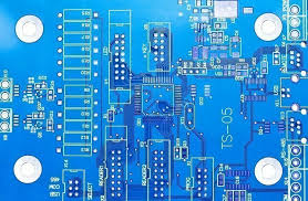
How to Maintain Thermal Management in a Radio Frequency Circuit Board
RF components require specific placement techniques to prevent signal degradation, which can lead to a variety of problems. Incorrect trace layouts, for example, create impedance discontinuities that increase losses. This can be caused by sharp turns in a trace or by crossing signals from different traces. These problems are typically worse at RF frequencies and must be avoided.
A good RF PCB will have an adequate amount of thermal vias to remove the heat generated by components and the conductive layer. The vias should be spaced correctly to prevent interference with the underlying components, and the plated through holes should be of a high quality to ensure reliable connections. This can be achieved by using a high-quality copper alloy in the drilled hole. A higher copper content will also improve the thermal conductivity of the hole and the PCB as a whole.
Component Placement: The placement of components on an RF circuit board is vital to ensuring the performance of the circuit. Components like resistors, capacitors, and inductors need to be placed in such a way that they minimize signal path lengths and avoid cross-talk between different components. Proper placement ensures that the signal flows smoothly through the circuit with minimal interference.
The materials used in RF PCB fabrication are crucial in determining the performance characteristics of the board. The most important properties of RF PCB materials are the dielectric constant (Dk), the loss tangent (Df), and the thermal stability. These properties affect signal integrity, attenuation, and heat dissipation. Common materials used for RF PCBs include: