
How Are Vias Involved in the RF Board Process?
Involved in the RF Board Process
In a multi-layered PCB, vias are used to connect traces and components on different layers of the board. They help with the distribution of power, signal routing, and grounding. There are several types of vias, including through-hole, blind, and buried. Each type has its own advantages and disadvantages. Through-hole vias are easily made but can cause parasitic inductance and capacitance, while blind and buried vias require a more complex manufacturing process but increase signal quality. Another type of via, called stitching vias, is used to connect multiple plane layers together. This structure is particularly useful in RF designs.
Vias are usually plated with copper, which conducts heat and signals. The plated copper also provides structural support to the via hole. This helps reduce the risk of shorts, corrosion, and other problems that can occur when the solder mask is applied to a unplated via. In addition, a plated via can be rerouted with ease when needed. Vias that are not used can be non-conductively filled or capped with a special material to prevent contaminants from entering the hole.
When designing a PCB, it is essential to specify the correct type of via and its treatment, as these will have an impact on the final product. A thorough specification will help avoid costly mistakes later on in the production phase. It is also important to know the exact dimensions of the via, as these will determine its positioning and size in the PCB layout.
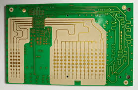
How Are Vias Involved in the RF Board Process?
Through-hole vias are the most common type of via. These holes run through all of the layers of a multi-layer PCB, connecting traces on the outermost layer and, if necessary, inner layers as well. They are more visible than blind or buried vias and can be spotted by the naked eye. Through-hole vias can be etched and plated with different materials, but the most common is pure copper.
Blind and buried vias are also known as microvias. These are smaller than through-hole vias and have a depth-to-diameter ratio of 1:1 or less. They are used to improve signal quality by reducing the distance between traces, which minimizes noise and EMI. They are typically plated with pure copper, but they can be etched and filled with non-conductive epoxy as well.
Stitching vias are used to make connections between the ground planes of multiple layers. This is crucial for high-speed and rf board where grounding can be critical to performance. Stitching vias can be etched or drilled, but they must be properly positioned and connected to prevent signal degradation.
When creating a multi-layer PCB, it is important to include vias in the design early on. This will ensure that all the traces are routed correctly and that any issues with the structure or layout can be resolved before manufacturing begins. It is also a good idea to create a library feature within the EDA software that will automatically generate instances of vias as the design progresses. This will save time during the routing stage and help to ensure that all the necessary requirements are met.